Shift Register: Classification and Working Principle

How Shift Registers Work?
Catalog
Ⅰ Introduction
In digital circuits, the circuits used to store binary data or codes are called registers. The register is a combination of flip-flops with a storage function. A flip-flop can store one bit of binary code, and then register that stores the N bit of binary code needs n flip-flops to form. According to its function, it can be divided into a basic register and a shift register.
The shift register is a sequential logic circuit that can be used to store or transmit data in the form of binary numbers. It loads the input data and then moves or "shifts" it to its output every clock cycle, so it is called a shift register. A shift register is basically composed of several single-bit "D-Latches", each data bit represents a logic "0" or "1", connected in a serial daisy-chain together, so that the output from one data latch becomes the input to the next latch.
The data in the shift register can be shifted bit by bit to the right or left under the action of the shift pulse. The data can be input in parallel, output in parallel, input in serial, output in serial, input in parallel, and output in serial, input in serial, output in parallel.
Shift registers can be used to register codes, and can also be used to implement the serial-parallel conversion of data, numerical operations, and data processing. Shift registers are used for data storage or data movement, so they are usually used inside calculators or computers. For example, two binary numbers can be stored before being added, or data can be converted from serial to parallel or parallel or parallel-serial format. The data latches that make up the shift register are all driven by a common clock (Clk) signal, making it a synchronous device.
There are many types of commonly used integrated shift registers, such as 74X164, 74X165, 74X166, 74X595 are eight-bit unidirectional shift registers, 74195 is four-bit unidirectional shift registers, 74194 is four-bit bidirectional shift registers, and 74198 is an eight-bit bidirectional shift register.

74LS674
Ⅱ Classification
According to the shift direction, it is often divided into three types: left shift register, right shift register, and bidirectional shift register;
The shift register can be used for data calculation and data processing, and realize the serial-parallel conversion of data. It can also be connected to various shift register counters, such as ring counters and twisted ring counters.
According to the input-output mode of shifted data, it can be divided into four circuit structures: serial input-serial output, serial input-parallel output, parallel input-serial output, and parallel input-parallel output.
(1) Serial input to parallel output (SIPO)-The register is loaded with serial data one bit at a time, and the stored data is provided in parallel at the output.
(2) Serial input to serial output (SISO)-The data is shifted serially on the "IN" and "OUT" of the register and shifted one bit at a time in the left or right direction under clock control.
(3) Parallel input to serial output (PISO)-Parallel data is loaded into the register at the same time, and is serially shifted out of the register one bit at a time under the clock control.
(4) Parallel input to parallel output (PIPO)-Parallel data is loaded into the registers at the same time, and transmitted to their respective outputs through the same clock pulse.
Ⅲ Principle of the shift register
The shift register can not only register data but also shift the data in it to the left or right in sequence under the clock signal.
The principle of the four-bit shift register: F0, F1, F2, and F3 are four edge-triggered flip-flops D, and the output Q of each flip-flop is connected to the input D of the flip-flop on the right. Because there is a delay from the rising edge of the clock signal CP is applied to the flip-flops until the new state of the output terminal is stably established, so when the clock signal is simultaneously applied to the four flip-flops, each flip-flop accepts the original data in the flip-flop on the left (input data D1 received by F0). The data in the register is shifted one bit to the right.

Four-bit shift register composed of D flip-flops
The shift register can move the stored data bit by bit to the left or right to achieve the required functions during the operation of the computer, see the picture:

4-bit serial input mobile register circuit schematic diagram
When starting, first add a clear pulse to the clear end to set the trigger output to 0. Then, the first data D0 is added to the serial input terminal of flip-flop 1, at the rising edge of the first CLK pulse, Q0=Q0, Q1=Q2. Q3=Q0. After that, the second data D1 is added to the serial input terminal. When the second CLK pulse arrives, Q0=Q1, Q1=Q0, Q2=Q3=0. By analogy, when the fourth CLK comes, each output terminal is Q0=Q3, Q1=Q2, Q2=Q1, Q3=Q0. The output data can be fetched in serial form or parallel open fetch.
From the perspective of logical structure, the shift register has the following two notable features: (1) The shift register is composed of the same register unit. Generally speaking, the number of register units is the number of bits of the shift register. In order to complete different shift functions, the connection between the output of each register unit and the input of the next adjacent register unit is also different. (2) All register units share a clock. Under the action of the common clock, the work of each register unit is synchronized. Each time a clock pulse is input, the data in the register moves one bit to the left or right in sequence. CMOS shift registers can usually be classified according to different data transmission methods. The data input mode of the shift register is divided into serial input and parallel input. Serial input is to send the input data from one input end to the register one by one under the action of a clock pulse; parallel input is to send the input data from several input ends to the register at the same time.
In CMOS shift registers, some varieties have only one input method of serial or parallel, but some varieties have both serial and parallel input methods. Serial input data is added to the D terminal of the first register unit, and input under the action of a clock pulse, the data transmission speed is slow; parallel input data is generally sent from the R and S terminals of the register unit, and the transmission speed is faster. The shift direction of the shift register is divided into the right shift and left shift. The right shift means that the data is input from the lowest bit on the left and output from the highest bit on the right in turn; when shifting to the left, the first bit on the right is the lowest bit, and the leftmost bit is the highest bit. The data is input from the right of the low bit and from the high bit. Output on the left.
The output of the shift register is also divided into serial and parallel. Serial output means that under the action of a clock pulse, the last output terminal of the register outputs the data of the register bit by bit; parallel output means that each register unit of the register has an output. Some varieties of CMOS shift registers have only one output method, but some varieties have both output methods. In fact, the parallel output mode must also have a serial output function.
Ⅳ To sum up
(1) A simple shift register can only use D-type flip-flops, one flip-flop for each data bit.
(2) The output of each flip-flop is connected to the D input of the right flip-flop.
(3) The shift register stores the data in the memory that is moved or "shifted" to its desired position in each clock pulse.
(4) Each clock pulse shifts the contents of the register one bit to the left or right.
(5) The data bits can be loaded one bit at a time in serial input (SI) configuration, or simultaneously loaded in parallel configuration (PI).
(6) For serial output (SO), data can be deleted from the register one bit at a time, or all data can be deleted from the parallel output (PO) at the same time.
(7) One application of shift registers is data conversion between serial and parallel or between parallel to serial.
(8) Shift registers are respectively recognized as SIPO, SISO, PISO, PIPO, or as general shift registers, combining all functions in a single device.
1.What is a shift register and its application?
The shift register is used as a Parallel to serial converter, which converts the parallel data into serial data. It is utilized at the transmitter section after the Analog to Digital Converter ADC block. The shift register is used as a Serial to parallel converter, which converts the serial data into parallel data.
2.What is the shift register and its types?
Shift Registers are sequential logic circuits, capable of storage and transfer of data. They are made up of Flip Flops which are connected in such a way that the output of one flip flop could serve as the input of the other flip-flop, depending on the type of shift registers being created. D-Flip Flop shift Register.
3.What is right shift register?
An n-bit shift register can be formed by connecting n flip-flops where each flip flop stores a single bit of data. The registers which will shift the bits to left are called “Shift left registers”. The registers which will shift the bits to right are called “Shift right registers”.
4.What is an 8-bit shift register?
The SN74HC595N is a simple 8-bit shift register IC. Simply put, this shift register is a device that allows additional inputs or outputs to be added to a microcontroller by converting data between parallel and serial formats. Essentially it takes 8 bits from the serial input and then outputs them to 8 pins.
5.Where are shift registers used?
Shift Registers are used for data storage or for the movement of data and are therefore commonly used inside calculators or computers to store data such as two binary numbers before they are added together, or to convert the data from either a serial to parallel or parallel to serial format.
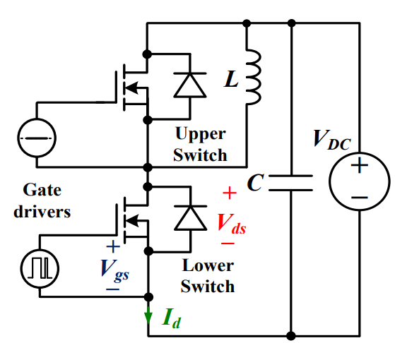
 Discovering New and Advanced Methodology for Determining the Dynamic Characterization of Wide Bandgap DevicesSaumitra Jagdale15 March 20242471
For a long era, silicon has stood out as the primary material for fabricating electronic devices due to its affordability, moderate efficiency, and performance capabilities. Despite its widespread use, silicon faces several limitations that render it unsuitable for applications involving high power and elevated temperatures. As technological advancements continue and the industry demands enhanced efficiency from devices, these limitations become increasingly vivid. In the quest for electronic devices that are more potent, efficient, and compact, wide bandgap materials are emerging as a dominant player. Their superiority over silicon in crucial aspects such as efficiency, higher junction temperatures, power density, thinner drift regions, and faster switching speeds positions them as the preferred materials for the future of power electronics.
Read More A Comprehensive Guide to FPGA Development BoardsUTMEL11 September 202514694
This comprehensive guide will take you on a journey through the fascinating world of FPGA development boards. We’ll explore what they are, how they differ from microcontrollers, and most importantly, how to choose the perfect board for your needs. Whether you’re a seasoned engineer or a curious hobbyist, prepare to unlock new possibilities in hardware design and accelerate your projects. We’ll cover everything from budget-friendly options to specialized boards for image processing, delve into popular learning paths, and even provide insights into essential software like Vivado. By the end of this article, you’ll have a clear roadmap to navigate the FPGA landscape and make informed decisions for your next groundbreaking endeavor.
Read More Applications of FPGAs in Artificial Intelligence: A Comprehensive GuideUTMEL29 August 20253607
This comprehensive guide explores FPGAs as powerful AI accelerators that offer distinct advantages over traditional GPUs and CPUs. FPGAs provide reconfigurable hardware that can be customized for specific AI workloads, delivering superior energy efficiency, ultra-low latency, and deterministic performance—particularly valuable for edge AI applications. While GPUs excel at parallel processing for training, FPGAs shine in inference tasks through their adaptability and power optimization. The document covers practical implementation challenges, including development complexity and resource constraints, while highlighting solutions like High-Level Synthesis tools and vendor-specific AI development suites from Intel and AMD/Xilinx. Real-world applications span telecommunications, healthcare, autonomous vehicles, and financial services, demonstrating FPGAs' versatility in mission-critical systems requiring real-time processing and minimal power consumption.
Read More 800G Optical Transceivers: The Guide for AI Data CentersUTMEL24 December 20253838
The complete guide to 800G Optical Transceiver standards (QSFP-DD vs. OSFP). Overcome supply shortages and scale your AI data center with Utmel Electronic.
Read More Xilinx FPGAs: From Getting Started to Advanced Application DevelopmentUTMEL09 September 20254299
This guide is your comprehensive roadmap to understanding and mastering the world of Xilinx FPGA technology. From selecting your first board to deploying advanced AI applications, we'll cover everything you need to know to unlock the potential of these remarkable devices. The global FPGA market is on a significant growth trajectory, expected to expand from USD 8.37 billion in 2025 to USD 17.53 billion by 2035. This surge is fueled by the relentless demand for high-performance, adaptable computing in everything from 5G networks and data centers to autonomous vehicles and the Internet of Things (IoT). This guide will walk you through the key concepts, tools, and products in the Xilinx ecosystem, ensuring you're well-equipped to be a part of this technological revolution.
Read More
Subscribe to Utmel !
![ATAES132A-MAHER-T]() ATAES132A-MAHER-T
ATAES132A-MAHER-TMicrochip Technology
![TLE8263EXUMA1]() TLE8263EXUMA1
TLE8263EXUMA1Infineon Technologies
![HCS365/P]() HCS365/P
HCS365/PMicrochip Technology
![HCS200/P]() HCS200/P
HCS200/PMicrochip Technology
![DLPA2005ERSLR]() DLPA2005ERSLR
DLPA2005ERSLRTexas Instruments
![ATSHA204-SH-CZ-T]() ATSHA204-SH-CZ-T
ATSHA204-SH-CZ-TMicrochip Technology
![SN74AVC6T622PWR]() SN74AVC6T622PWR
SN74AVC6T622PWRTexas Instruments
![MOC3061VM]() MOC3061VM
MOC3061VMON Semiconductor
![PAM8904JPR]() PAM8904JPR
PAM8904JPRDiodes Incorporated
![AD9961BCPZRL]() AD9961BCPZRL
AD9961BCPZRLAnalog Devices Inc.


 Product
 Brand
Brand Articles
 Tools
Tools


